- 您现在的位置:买卖IC网 > Sheet目录2003 > LTC1400IS8 (Linear Technology)IC A/D CONV 12BIT W/SHTDN 8-SOIC
LTC1400
13
1400fa
APPLICATIO S I FOR ATIO
W
U
In the Sleep mode, power consumption is reduced to a
minimum by cutting off the supply to all internal circuitry
includingthereference.Figure12showsthewaystopower
down the LTC1400. The chip can enter the Nap mode by
keeping the CLK signal low and pulsing the CONV signal
twice. For Sleep mode operation, CONV signal should be
pulsed four times while CLK is kept low.
The LTC1400 can be returned to active mode easily. The
rising edge of CLK will wake-up the LTC1400. During the
transition from Sleep mode to active mode, the VREF volt-
age ramp-up time is a function of the loading conditions.
With a 10μF bypass capacitor, the wake-up time from
Sleep mode is typically 4ms. A REFRDY signal will be
activated once the reference has settled and is ready for
an A/D conversion. This REFRDY bit is output to the DOUT
pin before the rest of the A/D converted code.
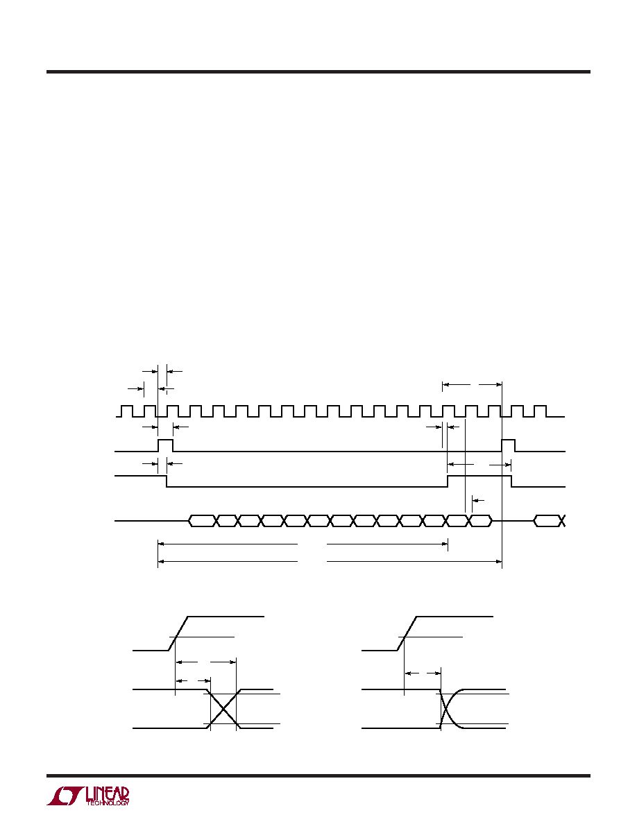
Digital Interface
The digital interface requires only three digital lines. CLK
and CONV are both inputs, and the DOUT output provides
the conversion result in serial form.
Figure 13 shows the digital timing diagram of the LTC1400
during the A/D conversion. The CONV rising edge starts
the conversion. Once initiated, it can not be restarted until
the conversion is completed. If the time from CONV signal
to CLK rising edge is less than t2, the digital output will
be delayed by one clock cycle.
The digital output data is updated on the rising edge of the
CLK line. DOUT data should be captured by the receiving
system on the rising CLK edge. Data remains valid for a
minimum time of t10 after the rising CLK edge to allow
capture to occur.
CLK
CONV
INTERNAL
S/H STATUS
DOUT
t7
t3
1
2
3
4
5
6
7
8
9
10
11
12
13
14
15
1
2
t2
t6
t4
t5
t8
tACQ
SAMPLE
HOLD
Hi-Z
tCONV
tSAMPLE
1400 F13
REFRDY D11
D9
D8
D7
D6
D5
D4
D3
D2
D1
D0
D10
REFRDY
Figure 13. ADC Digital Timing Diagram
Figure 14. CLK to DOUT Delay
t10
t8
VIH
VOH
VOL
DOUT
CLK
t9
VIH
90%
10%
DOUT
CLK
1400 F14
发布紧急采购,3分钟左右您将得到回复。
相关PDF资料
LTC1401IS8#TRPBF
IC A/D CONV 12BIT W/SHTDN 8-SOIC
LTC1402IGN#TRPBF
IC ADC 12BIT 2.2MSPS SHDN 16SSOP
LTC1403AHMSE#TRPBF
IC ADC 14BIT 2.8MSPS DIFF 10MSOP
LTC1403AIMSE-1#TRPBF
IC ADC 14BIT 2.8MSPS DIFF 10MSOP
LTC1404IS8#TRPBF
IC A/D CONV 12BIT W/SHTDN 8-SOIC
LTC1405IGN#TRPBF
IC ADC 12BIT 5MSPS SAMPLE 28SSOP
LTC1406IGN#TRPBF
IC A/D CONV 8BIT SAMPLING 24SSOP
LTC1407AHMSE#PBF
IC ADC 14BIT 3MSPS 10-MSOP
相关代理商/技术参数
LTC1400IS8#PBF
功能描述:IC A/D CONV 12BIT W/SHTDN 8-SOIC RoHS:是 类别:集成电路 (IC) >> 数据采集 - 模数转换器 系列:- 标准包装:1 系列:microPOWER™ 位数:8 采样率(每秒):1M 数据接口:串行,SPI? 转换器数目:1 功率耗散(最大):- 电压电源:模拟和数字 工作温度:-40°C ~ 125°C 安装类型:表面贴装 封装/外壳:24-VFQFN 裸露焊盘 供应商设备封装:24-VQFN 裸露焊盘(4x4) 包装:Digi-Reel® 输入数目和类型:8 个单端,单极 产品目录页面:892 (CN2011-ZH PDF) 其它名称:296-25851-6
LTC1400IS8#TR
功能描述:IC ADC 12BIT 400KSPS SHTDN 8SOIC RoHS:否 类别:集成电路 (IC) >> 数据采集 - 模数转换器 系列:- 标准包装:1,000 系列:- 位数:16 采样率(每秒):45k 数据接口:串行 转换器数目:2 功率耗散(最大):315mW 电压电源:模拟和数字 工作温度:0°C ~ 70°C 安装类型:表面贴装 封装/外壳:28-SOIC(0.295",7.50mm 宽) 供应商设备封装:28-SOIC W 包装:带卷 (TR) 输入数目和类型:2 个单端,单极
LTC1400IS8#TRPBF
功能描述:IC A/D CONV 12BIT W/SHTDN 8-SOIC RoHS:是 类别:集成电路 (IC) >> 数据采集 - 模数转换器 系列:- 标准包装:1,000 系列:- 位数:16 采样率(每秒):45k 数据接口:串行 转换器数目:2 功率耗散(最大):315mW 电压电源:模拟和数字 工作温度:0°C ~ 70°C 安装类型:表面贴装 封装/外壳:28-SOIC(0.295",7.50mm 宽) 供应商设备封装:28-SOIC W 包装:带卷 (TR) 输入数目和类型:2 个单端,单极
LTC1400IS8PBF
制造商:Linear Technology 功能描述:ADC SAR 400ksps 12-Bit Serial SOIC8
LTC1401CS8
功能描述:IC A/D CONV 12BIT W/SHTDN 8-SOIC RoHS:否 类别:集成电路 (IC) >> 数据采集 - 模数转换器 系列:- 标准包装:2,500 系列:- 位数:16 采样率(每秒):15 数据接口:MICROWIRE?,串行,SPI? 转换器数目:1 功率耗散(最大):480µW 电压电源:单电源 工作温度:-40°C ~ 85°C 安装类型:表面贴装 封装/外壳:38-WFQFN 裸露焊盘 供应商设备封装:38-QFN(5x7) 包装:带卷 (TR) 输入数目和类型:16 个单端,双极;8 个差分,双极 配用:DC1011A-C-ND - BOARD DELTA SIGMA ADC LTC2494
LTC1401CS8#PBF
功能描述:IC A/D CONV 12BIT W/SHTDN 8-SOIC RoHS:是 类别:集成电路 (IC) >> 数据采集 - 模数转换器 系列:- 标准包装:1 系列:microPOWER™ 位数:8 采样率(每秒):1M 数据接口:串行,SPI? 转换器数目:1 功率耗散(最大):- 电压电源:模拟和数字 工作温度:-40°C ~ 125°C 安装类型:表面贴装 封装/外壳:24-VFQFN 裸露焊盘 供应商设备封装:24-VQFN 裸露焊盘(4x4) 包装:Digi-Reel® 输入数目和类型:8 个单端,单极 产品目录页面:892 (CN2011-ZH PDF) 其它名称:296-25851-6
LTC1401CS8#TR
功能描述:IC ADC 12BIT 200KSPS SHTDN 8SOIC RoHS:否 类别:集成电路 (IC) >> 数据采集 - 模数转换器 系列:- 标准包装:2,500 系列:- 位数:16 采样率(每秒):15 数据接口:MICROWIRE?,串行,SPI? 转换器数目:1 功率耗散(最大):480µW 电压电源:单电源 工作温度:-40°C ~ 85°C 安装类型:表面贴装 封装/外壳:38-WFQFN 裸露焊盘 供应商设备封装:38-QFN(5x7) 包装:带卷 (TR) 输入数目和类型:16 个单端,双极;8 个差分,双极 配用:DC1011A-C-ND - BOARD DELTA SIGMA ADC LTC2494
LTC1401CS8#TRPBF
功能描述:IC A/D CONV 12BIT W/SHTDN 8-SOIC RoHS:是 类别:集成电路 (IC) >> 数据采集 - 模数转换器 系列:- 标准包装:2,500 系列:- 位数:16 采样率(每秒):15 数据接口:MICROWIRE?,串行,SPI? 转换器数目:1 功率耗散(最大):480µW 电压电源:单电源 工作温度:-40°C ~ 85°C 安装类型:表面贴装 封装/外壳:38-WFQFN 裸露焊盘 供应商设备封装:38-QFN(5x7) 包装:带卷 (TR) 输入数目和类型:16 个单端,双极;8 个差分,双极 配用:DC1011A-C-ND - BOARD DELTA SIGMA ADC LTC2494